Theory of Auger electron spectroscopy
Introduction
Auger electron spectroscopy (AES) has now emerged as one of the most widely used analytical techniques for obtaining the chemical composition of solid surfaces. The basic advantages of this technique are its high sensitivity for chemical analysis in the 0.4 to 5nm region near the surface, a rapid data acquisition speed, its ability to detect all elements above helium, and its capability of high-spatial resolution. The high-spatial resolution is achieved because the specimen is excited by an electron beam that can be focused into a fine probe with ultra-high vacuum (UHV) technology.
Basic Principle
Auger Effect - Underlying the AES technique is the Auger effect, which was discovered by Pierre Auger in 1925. Fig. 1 shows the illustration of Auger spectroscopy using the K, LI & LII,LIII levels. These could be the inner core levels of an atom in either a molecular or solid-state environment. The Auger process is initiated by creation of a core hole, which is typically carried out by exposing the sample to a beam of high energy electrons (typically having a primary energy in the range 2 - 20keV). Such electrons have sufficient energy to ionize all levels of the lighter elements, and higher core levels of the heavier elements. Ionization is shown to occur by removal of a K-shell electron, but in practice such a crude method of ionization will lead to ions with holes in a variety of inner shell levels. The ionized atom that remains after the removal of the core hole electron is, of course, in a highly excited state and will rapidly relax back to a lower energy state. One electron falls from a higher level to fill an initial core hole in the K-shell and the energy liberated in this process is simultaneously transferred to a second electron; a fraction of this energy is required to overcome the binding energy of this second electron, the remainder is retained by this emitted Auger electron as kinetic energy.
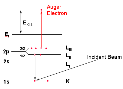 Fig.1 - The diagram showing the Auger effect
Below Fig. 2 is a cross-section of the paths of electron in the optics column with coaxial Cylindrical Mirror Analyzer (coaxial CMA). AES can have spectrum Survey, Line Scan, Mapping and depth profile analysis with ion gun sputtering. There are two kinds of analyzer for Auger electron signal, Spherical Capacitor Analyzer (SCA) and Cylindrical Mirror Analyzer. CMA has two main advantages over SCA: (1) when electron beam is coming at a tilt angle with sample, CMA still can get strong signal to keep high sensitivity. (2) With the 360-degree data acceptance angle, high intensity can be kept with smallest possible spatial resolution. Hence such as Auger map from the CMA could be much clearer than that from a SCA.
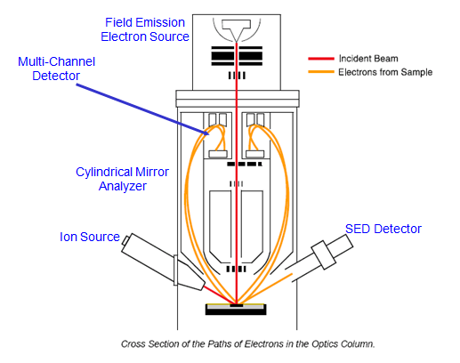 Fig. 2 - The cross section of the paths of electron in the optics column with coaxial CMA
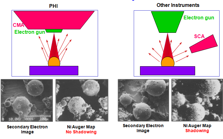 Fig. 3 - The SEM image and Auger map comparison between CMA and SCA
Application of AES
Example 1 - Fig. 4 shows Ga Auger map and SEM image of 10nm GaAs/ AlAs super lattice structure. The 500kX SEM image and Ga map show excellent resolution of the 10nm layers.
(a) (b)
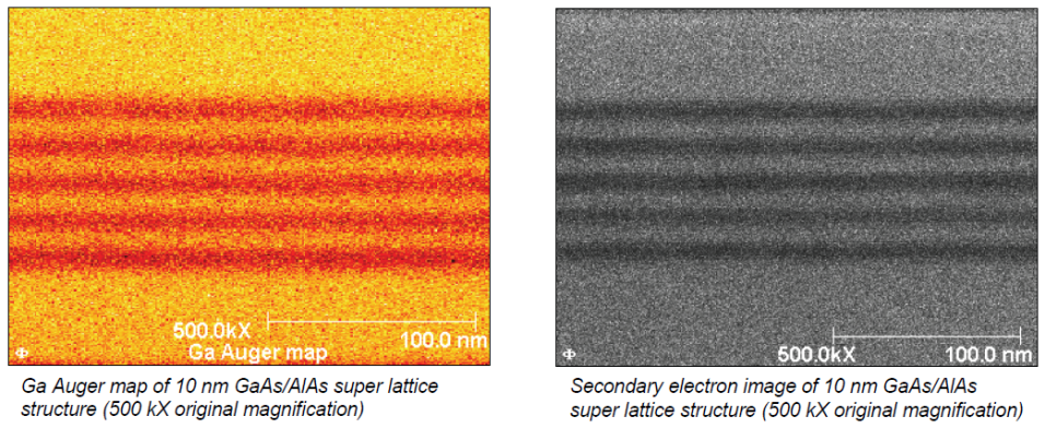
Fig. 4 (a) Ga Auger map of 10 nm GaAs/AlAs super lattice structure. (b) SEM image of 10 nm GaAs/AlAs super lattice structure
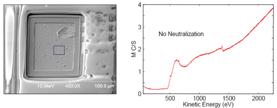
Example 2 - Besides, Auger analysis of insulating materials can be impeded by the sample charging to a high negative surface potential. This surface charge severely distorts and shifts secondary electron spectra, which includes the Auger electron peaks, rendering the Auger data meaningless. Fig. 5 shows a 70eV Ar+ ion beam was used during Auger analysis to eliminate the charge on the polyimide surrounding the bond pad. This made it possible to obtain a normal Auger spectrum from the bond pad.
| (a) | (b) | (c) | |
 |
 |
||
| Fig. 5 - Auger spectrum with low energy ions of charge Neutralization. (a) Analysis Al bonding pad surrounded by polyimide (b) Auger spectrum without Neutralization (c) Auger spectrum with Neutralization | |||
Example 3 - In order to get better energy resolution, PHI 700Xi AES provide from 0.5% to 0.05% energy resolution. Fig. 6 shows AES spectrum on Al foil. Normal AES only can resolve Al2O3 1386.9 eV peak, but PHI 700Xi can resolve 1393.4eV peak metal state of Al. This ultra high resolution provides us possible to observe chemical binding status by AES.
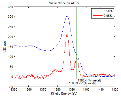 Fig. 6 - Ultra high energy resolution on Al foil by PHI 700Xi AES
Summing-up
Auger Electron Spectroscopy (AES) is a surface-sensitive spectroscopic technique used for elemental analysis of surfaces; it offers:
1) high sensitivity for all elements except H and He,
2) a means of monitoring surface cleanliness of samples and
3) quantitative compositional analysis of the surface region of specimens, by comparison with standard samples of known composition.
Now AES is widely applied in semiconductor, metallurgy, catalyst, corrosion, glass, crystal and interface research.
For more details, please visit our Brochure or Application Notes.

